EECS 373 : Libero SoC v11.7 Tool Flow Reference Guide
9/1/2016
Actel Libero is an Integrated Development Environment (IDE) used to
configure the SmartFusion chip on your kit.
This is a beginning guide to create a project flow within Libero to
develop
custom hardware for the FPGA and configure Micro-controller SubSystem
(MSS).
The guide consists of the following sections.
- Project Tutorial for Lab 1
- Creating a Project
- Creating Custom Hardware in the FPGA
- Modifying an Existing Design
- Adding a Clock Source to the FPGA
- FPGA Pin Out Reference
- Common Tool Pitfalls
Tool Flow Tutorial for Lab 1
The Libero SoC Project Manager organizes the SmartFusion
hardware
development
tool chain with an intuitive GUI. Libero SoC is installed on the 373
workstations. Libero SoC is also available free from Actel Microsemi
at this link
with all the
functionality required for the course. SoC is currently NOT available
on CAEN loads.
Part 1: Project Creation
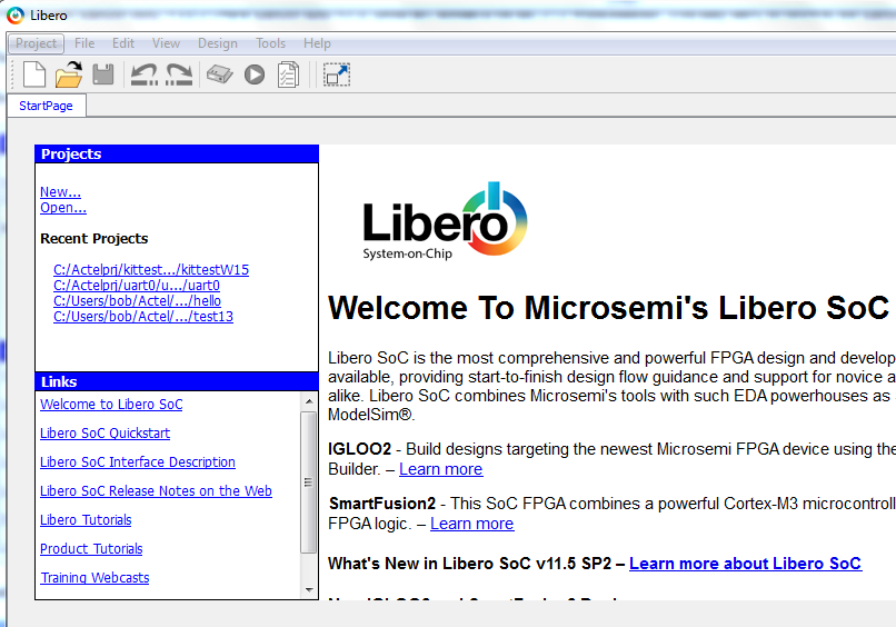
Open the Libero Project Manger Libero SoC V11.7.
Libero should then open with the
following start page.
Naming the Project and Location
Under Projects, select
new and the following window will appear.
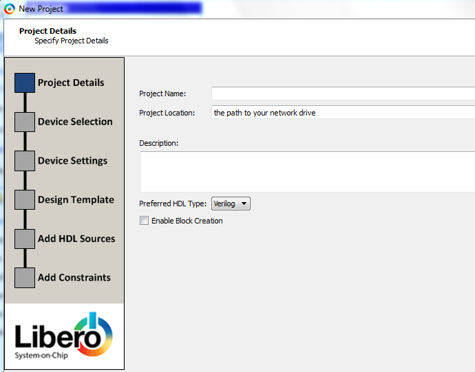
This window will allow us to
name the project and locate it.
Project Name:
andor
Project Location:
You may locate your
project in several places. You can put in your user space for this
workstation, but you will only have access to it on that computer or
you can put it in your UoM directory space (engin-labs.m.storage..etc).
The directory should be
automatically mapped to the logon unique name. You should see a drive
letter associated with it. If it is not, you can map it by opening
Computer and clicking on the heading Map Network Drive. Add the path
\\engin-labs.m.storage.umich.edu\uniqname.
There is no need to create a project folder. Libero will automatically
create a project folder at the specified location with the project
name. In this case, a folder named andor will automatically
be
created. Caution: Do not use spaces in the
directory folder names.
Preferred HDL Type: This should be set to Verilog.
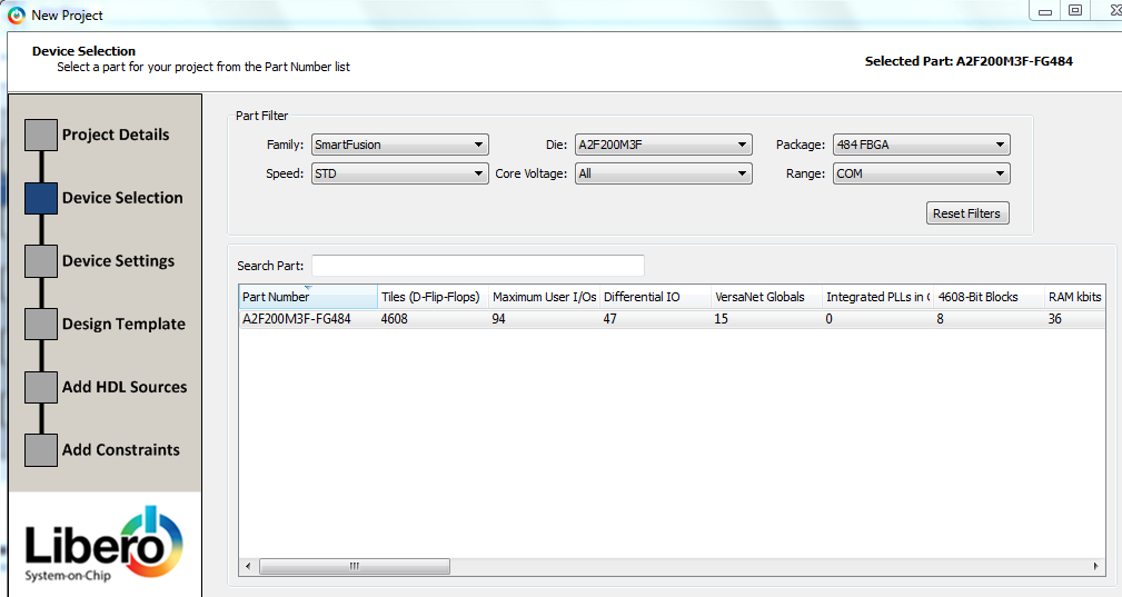
Setting the Device Type
Click next and you should see the following window.
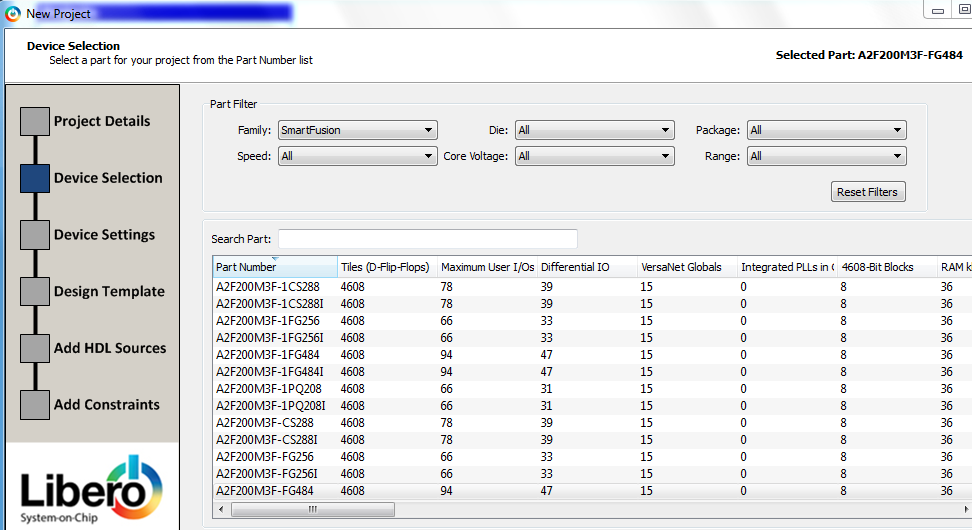
Select the following fields.
Family:
SmartFusion
Die:
A2F200M3F
Package:
484FBGA
Speed: STD
Core Voltage: All
Range: COM
The settings should look like this after you are finished with the A2F200M3F-FG484 the remaining part choice.
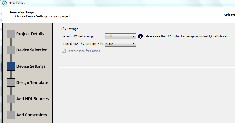
Device Settings
Click next to advance to device settings. The
following page should appear with these settings. If not, select these
settings.
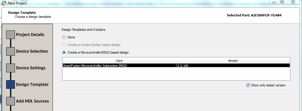
Design Template
Click next to advance to device settings. The
following page should appear. This option allows you to include the
integrated ARM processor and its peripherals in your design.
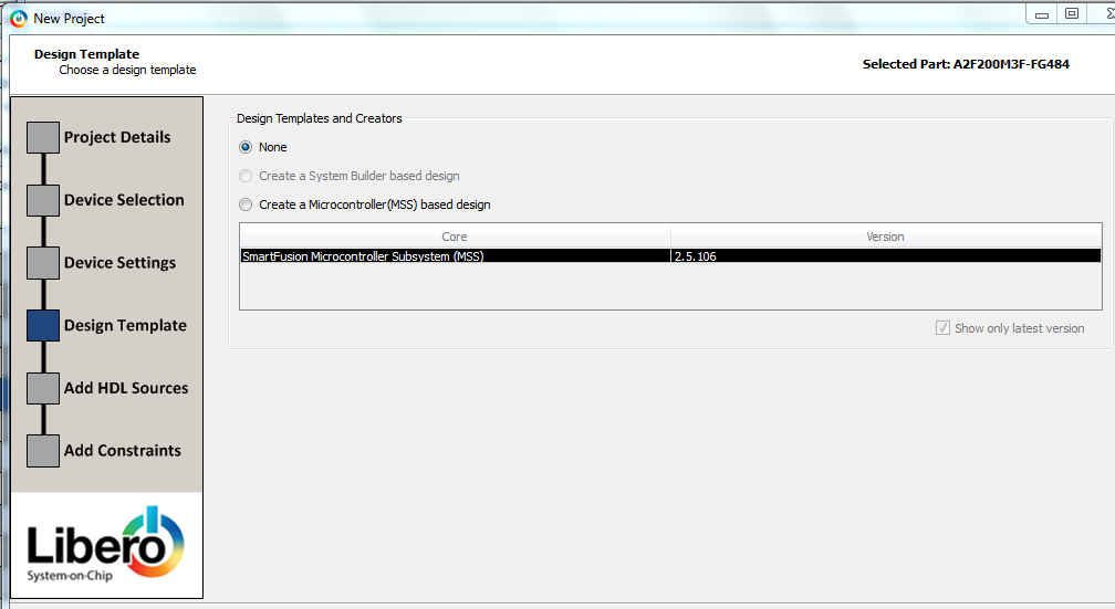
Select Create a Microcontroller(MSS) based design.
You will use this feature in all your labs.
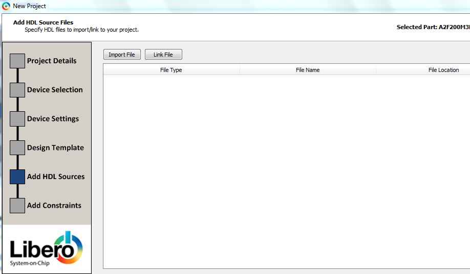
Add HDL Sources
Click next to advance to device settings. The following page should appear. There are no sources files to add.
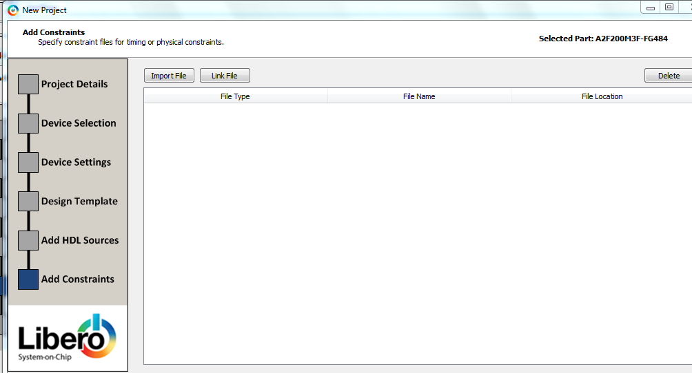
Add Constraints
Click next to advance to Add Constraints. The following page should appear. There are no constraints to add.
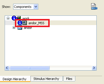
Project Start Page
Click Finish and the following page should appear.
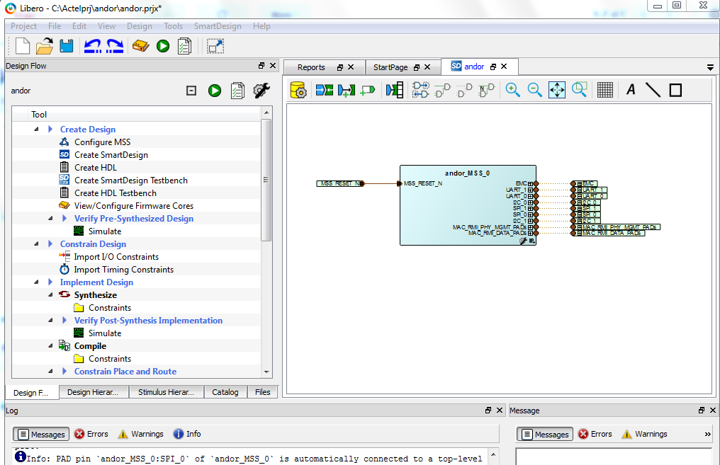
The instantiated block andor_MSS_0 represents all the peripherals
associated with ARM processor and potential connections to the ARM
processor buses. In addition, it is possible to add other hardware
components that will be instantiated in the FPGA. These components may
be custom designs or standard components that are available in the
catalog.
The upper left pane displays the project directory and associated
files. At this point we only have a project directory.
The mid left pane shows the status of the design flow. It includes all
the basic steps in the design flow process. If we collapse all
the
tools we can see them all as follows.
Design
Entry: FPGA hardware can
be designed using typical HDLs such as Verilog.
Constrain
Design: FPGA pin
assignments files are imported with this tool. Note we will actually
provide the FPGA pin constraints using an editor under the
Implement Design heading
with a convenient editor.
Implement
Design: Synthesize
design descriptions and generate programming files for the specific
FPGA device.
Program
Design: Programs or
configures the FPGA.
Debug
Design: Can be used to
insert specialize debugging hardware. We will not use this tool.
Handoff
Design for Production:
Optimizes design for production removing debug tools and files.
Develop
Firmware: This tool
will evoke the software development tool (SoftConsole) and
automatically import device libraries.
In a typical design build, these tools will run in the
background flowing from one tool to the next. You can see the scripts
running in the Log or console window in the bottom pane. Any of the
Design Flow tools can be run manually by right clicking on the tools
and selecting run interactively. Report files are also generated for
each one of these tools and are accessible under each heading. These
can be useful to debug your design.
Finally the top right pain shows the current design as a graphic. The
graphic represents basic system IO devices such as Ethernet
ports,
custom hardware modules and interfaces to the ARM processor.
When a new project is created, the project manager creates a design
that includes a number of IO pins connected to a large block.
This block is referred to as the MSS or Microprocessor SubSystem.
Double clicking on the MSS will open a graphic representation of
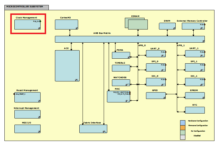
all the system subcomponents. It will look like this.
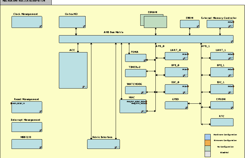
Components can be added or removed via their associated check box.
Also, some
components can be specifically configured by double clicking them. We
won't be using this in this tutorial, so close this window and return
to the andor project view. Highlight the MSS, the connected pins
and delete them.
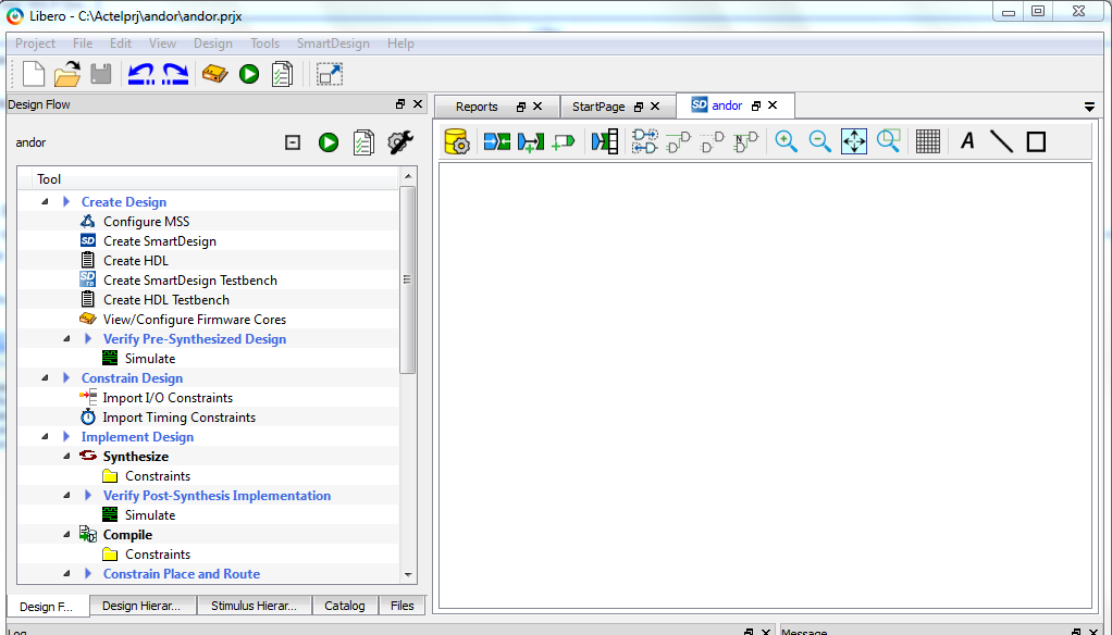
Close this window, save the changes and return to the andor project view. The project window will look like this.
Edit Tool Profile
There is one last step we need to do before starting our design
example. For this step we need to specify the directory path to a
software tool that we will use in future labs. Although we aren't using
it yet, it will report errors
if we don't specify the path.
Under the Project menu, click on Tool Profiles. The following
window should open.
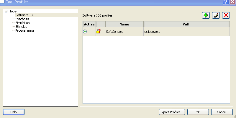
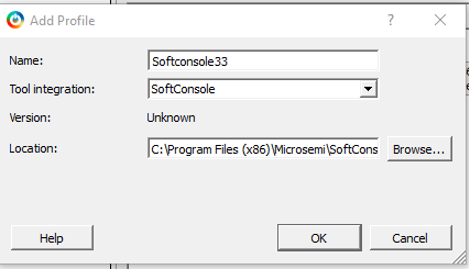
We will add a path to the SoftConsole 3.3 executable. Click the green +
button upper right corner. Add the name SoftConsole33. Add the
tool integration SoftConsole. Add the following path in location or
browse to C:\Program Files (x86)Microsemi\SoftConsolev3.3\Eclipse\eclipse.exe
The final project tool window should look like this.

Part 2: Adding a Custom
Hardware Component to the System
Design Entry
For this tutorial we will add a custom hardware component to our
design. It will have the function illustrated in the
following schematic.
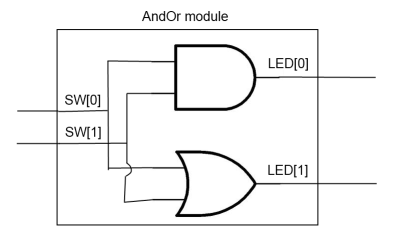
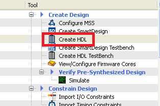
We will express the design in Verilog. To enter a Verilog file, select
Create HDL under Create Design in the tool flow pane.
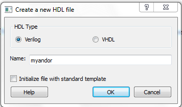
The following window will appear. Make sure Verilog is selected,
un-check initialize standard Verilog format and name the file
myandor. The window should look like this. Press OK. Note we cannot
name the file andor since the project name is andor. If you do, an
error will be generated when you save the file.
The file andor.v will be opened. Put the following Verilog code in the
file. Note, there is a syntax error and synthesis error for the sake of
demonstrating the file checking tools.
module myandor (

input[1:0] SW,
output wire [1:0] LED
             );

assign LED = SW[0] & SW[1]; //And
assign LED = SW[0] | SW[1] //Or

endmodule
Save the file.
The code we provided has a simple syntax error. To check syntax, right
click in the Verilog file window and select check HDL.
The console window will indicate an error and identify the
line number. Fix the bug, save the file and check the syntax.
There is one more bug that is not a syntax error. We will use
the synthesizer to find this bug below.
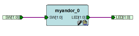
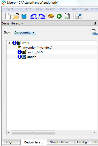
Next we must instantiate Verilog module in the design. In the Design
Hierarchy pane (tab), select myandor.v and drag it into the andor design
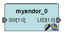
window. The Verilog file myandor will have the following graphic
representation in the window.
We have just one more bit of of design entry to complete
before synthesizing this Verilog. The ports of myandor must be promoted
to the the top level so they can be connected to FPGA pins. For each
port, right click and select promote to top level.
Your design should look like this when complete.
The project andor should be set as
the root design file (top level). To do so, select andor in the
Design Hierarchy view, right click and set as root.
If it is already set to the
root, it will appear in bold and there will be no choice to set it as
the root or top level.
Finally, save project by clicking on the save file icon. Note, you will
notice a * next to any file tab that is not saved.
Synthesis
Next we will synthesize the the design. Before we can do that we have
to "Generate" the design entry. To generate, double click the  icon.
icon.
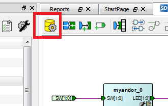
In the Log window you should see a message indicating andor is
successfully generated.
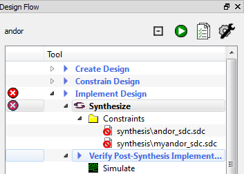
Under Implement Design in the Design Flow pane, double click on
Synthesis. There is still one error left in our design so it will fail.
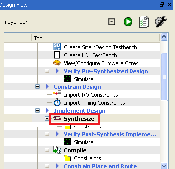
You will see an activity symbol
to the left of the Synthesize line. You may be prompted to grant access
through the firewall. You can acknowledge or cancel. If synthesis was
successful, a
check mark will appear to the left of the Synthesize line. You will
notice that under Synthesize--> Constraints in the Design Flow
pane that there is a warning indicated next to the sdc file. This is
because we did not include a pin constraint file. We will add the pin
constraints later.
If an error occurred during
synthesis, a red symbol will occur next to the synthesize line. It will
look something like this.
You can examine the reports
file tab in the upper left pane for hints or open the synthesizer in
interactive mode. This can be very helpful. Synthesis errors and subtle
problems associated with warning are very typical problems in the
lab.
Lets take a look at this case. To open the synthesizer in manual mode,
select Synthesize, right click and select Open Interactively. This will
open the Synplify Pro application. It will look something like this.
You may have to expand the files listed under Verilog in the
directory window.
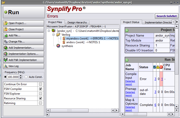
Notice that errors and warning
are associated with myandor.v. Select this file and open by double
clicking. The following window will open.
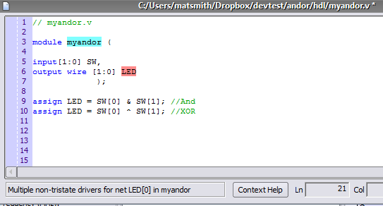
The red highlighted Verilog
indicates the error. If you select this error, the error
description is indicated in the bottom left window. In this case it is
"Multiple non-tristate drivers for net LED[0] in myandor". This is a
bit cryptic, but if you look closely at the LED assignments you
will notice that member or LED number is not specified. The first LED
assignment should be assigned to LED[0] and the 2nd assignment should
be assigned to LED[1]. In
some cases you will receive warning highlighted in yellow. Be sure to
check these too and make sure they are warnings of no consequence. The
blue highlight on mayandor is just an activity indicator and
is not associated with errors.
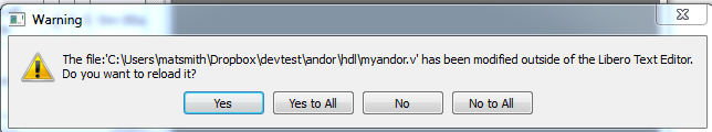
You can fix this error in the Synplify editor window, save it and
synthesize by hitting RUN on the Synplify project page. In this way you
can check your correction. The Libero Project manager will ask if you
want to update project files such as myandor. Agree to the update. The
prompt will look like this for instance.
Close Synplify. You should notice that the Synthesize line in the
Design Flow pane has a green check next to it.
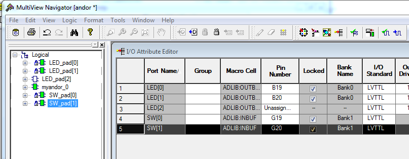
Assigning FPGA Pins
Next we must assign the switches, LEDs and test points to devices on
the kit. The FPGA pins associated with these devices are listed below
for your convenience. A complete list of all the
devices and their associated FPGA pins are in a document linked with
PIN OUT quick reference below.
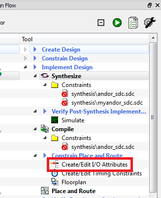
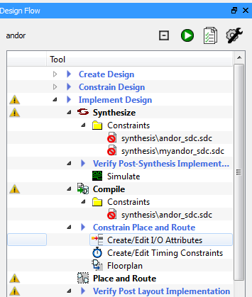
To make the assignments, we need to double click on "Create/Edit IO
Attributes" under Implement Design--> Compile-->Constrain
Place and Route in the Design Flow of the Libero Project Manager as
shown below.
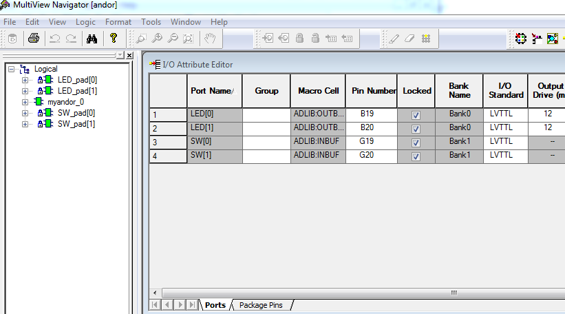
This will initiate the Compile process and open the Designer
application in a new window. Designer has many parts, with
the IO Attribute Editor opening for pin entry. You will see your port
name listed for the andor function. Under the Pin Number column set the
pins according to the FPGA pin specification listed at the end of this
document. Simply click on the Pin Number window and select the pin
number. It should look like the following window when you are
complete.
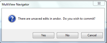
Close this window. You will be asked to commit the design.
Confirm by clicking yes.
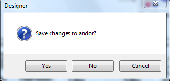
Now close the Designer Window. You will asked if you want to save the
changes. Confirm by clicking yes.
Programming the FPGA
Finally you must program the FPGA. Be sure that both USB
cables of your
kit are connected to your workstation. To
start the
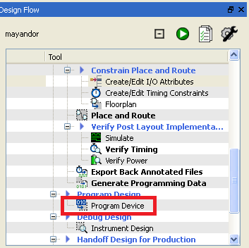
programming process select Program Device under Program Design in the
Design Flow pane in the Libero Project Manager.
The Libero Project Manager will
complete all the dependencies required to program the device such as
Place and Route and generation of the programming files. You will see
the activity indicators as the design flow advances. This
process can take several minutes to complete. Some warning may be
generated for the post layout and timing verification in the
Place and Route. You can ignore these.
Once the Programing of the FPGA
starts the following notice will be displayed. This part will take
awhile (1-2 minutes). On the board, there will be a flashing yellow LED
while the device is programming. When it completes, a green LED will
turn on next to it.
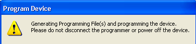
When this dialog disappears, the process is complete. You
should see
green check marks next to all the Design Flow from Design Entry to
Program Device.
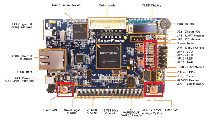
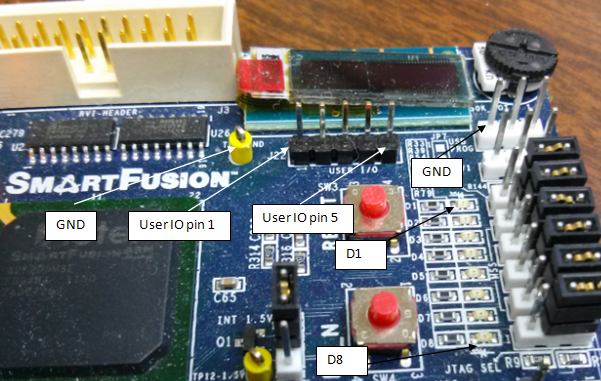
Verify the operation of the logic by observing the LEDs as you activate
the switches. The kit with the identified devices is provide here for
your convenience.
User LEDs 0 and 1 (top right) should activate when pressing user switch
1 and 2 (lower left and right). Header J22 (upper left)
provides the connection to the test points. These can be observed with
a scope or logic analyzer.
Keep in mind the switches and
LEDs are active low. That is, the switch
creates zero when pushed and the led illuminates when a logical 0 is
applied.
Summary
- Start a project
- Enter a design in an HDL file
- Instantiate the the design in the top level (project)
- A syntax check will occur automatically when you instantiate.
- Set the project as the ROOT or top level
- Generate the top level
- Create/Edit IO Attributes
- Synthesis will be be automatically evoked. If there are errors
consider running manually to correct.
- If you do not have to enter pin constraints, you can go
directly to Program Device
- Program Device
- While the board is programming, a yellow led in the upper left
corner will blink. When it is finished it will turn green.
Synthesis, Place and Route and Programming the FPGA can take 1-2
minutes each. If it take more than 3-4 minutes, something is probably
wrong and you will probably have to use the task manager to halt the
process.
The Libero SoC windows can take a bit of time to update. You may have
to wait for the Design Flow window to update status of the tools or an
instance in the top level design may take a moment to update.
Part 3: Modifying a Custom
Hardware Component
Lets consider a few cases of modifying the design and see how to use
the Design Flow to do this.
Case 1
Lets consider changing the original Verilog file so that
LED 1 is equal to the exclusive OR of the switches 1 and 2 instead of
the or of the switches. Select the Verilog file tab myandor and modify
the assignment line to be an exclusive OR as follows.
module myandor (

input[1:0] SW,
output wire [1:0] LED
             );

assign LED[0] = SW[0] & SW[1]; //And
assign LED[1] = SW[0] ^ SW[1]; //XOr

endmodule
Save the file and the Project Manager should update the status in the
Design Flow window. It should look something like this.
To update the design to the FPGA all that is needed is to generate and Double Click
on Program Device under Program Design in the Design Flow. You
will notice the Design Flow process will proceed through each step.
Green
check marks should appear for each step.
You can check to see if LED 1 now exhibits and XOR function.
Summary
In this case you need only evoke the following tools in this
order.
- Editor: Modify your Verilog
- Generate: Build the Top Level Design
- Program FPGA: Program Device
Case 2
Lets consider what we need to do if we want to add some more IO. Lets
add the OR function back assigning it to LED2. Open the Verilog file
myandor and add the assignment for LED 2. The Verilog should look
something like this.
module myandor (

input[1:0] SW,
output wire [2:0] LED
             );

assign LED[0] = SW[0] & SW[1]; //And
assign LED[1] = SW[0] ^ SW[1]; //XOr
assign LED[2] = SW[0] | SW[1]; //XOR

endmodule
Save the file. Open the project design tab andor. You should notice a
warning associated with myandor symbol. It will appear like this.
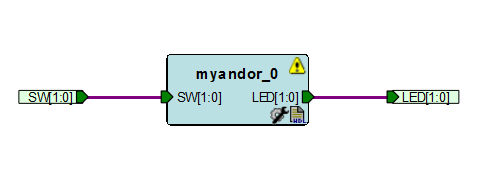
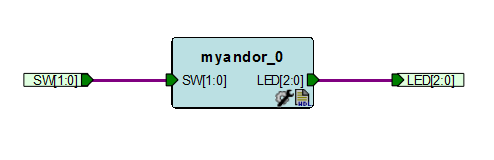
Since we added another LED port, the symbol will have to be updated.
Right click on the symbol and select "Update Instance(s)
with Latest Component". The LED
connector LED[1:0] should disconnect. Delete LED[1:0], select LED port
LED[2:0], right click and promote to top level. It should look
like this when you are finished.
The choice to
update the instance will not be available if there is a snytax
error in your Verilog. Go back to your file and run check syntax as
necessary.
Save this file and generate.
You will have to add the pin constraint for LED 2. Double click
"Create/Edit IO
Attributes" under Implement Design--> Compile-->Constrain
Place and Route" in the Design Flow as you did above. The
following
window will open.
Add the appropriate pin number for LED 2. The FPGA pin numbers for
the LEDs are listed at the end of this document.
As we did earlier, close this window and acknowledge the commit and
save of this pin change. Close the Designer window and acknowledge the
save as needed.
Now click on Program Device.
Summary
In this case you need only evoke the following tools in this
order.
- Editor: Modify your Verilog
- Generate: Build the Top Level Design
- Constraint Editor: Add pn assignment
- Program FPGA: Program Device
Part 4: Adding a Fabric Clock
To design sequential logic we will need a clock. In this section we
show you how to add a clock to the FPGA. Lets consider adding some
simple logic that counts transitions of SW0. We will use a 3-bit
counter to accumulate the counts and display the output on LEDs 3-5.
SW1 will be used to clear the counter. You will notice that we run SW0
through a series of 2 DFFs. It is important and common practice to
synchronize an asynchronous event such as a switch transition with the
system clock.
Modify your myandor Verilog file to include the
following code. You will have to update the myandor instance in the top
level design view and connect a expanded LED connector.
module myandor (
input clk,
input[1:0] SW,
output wire [5:0] LED
             );

assign LED[0] = SW[0] & SW[1]; //And
assign LED[1] = SW[0] ^ SW[1]; //XOr
assign LED[2] = SW[0] | SW[1]; //XOR

reg Q0, Q1, Q2;
//synchronize SW0 to the system clk with two flipflops connected in series
always@(posedge clk)
begin
Q0 <= SW[0];
Q1 <= Q0;
end

//count switch transitions
reg[2:0] count;
always@(posedge Q1)
begin
if (~SW[1])
   count <=0;
else
   count <= count +1;
end

assign LED[3] = ~count[0];
assign LED[4] = ~count[1];
assign LED[5] = ~count[2];
endmodule
The clock source is
associated with the andor_MSS_0 instance that we previously removed. We
will have to add it back to our top level design. Select andor_MSS in
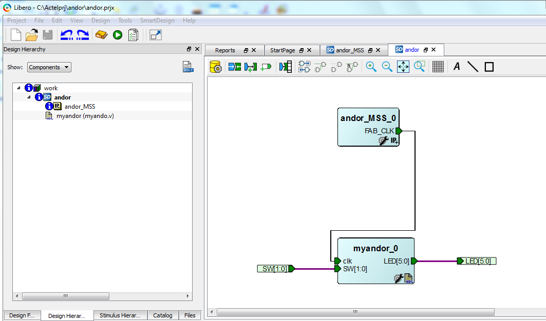
the Design Hierarchy window as shown below.
Right click and select
"instantiate" in andor.
The design pane should look
like this with both
instances in the design window. The clk port is not connected yet. We will have to provide a clock source from the andor_MSS_0.
Double click on
the andor_MSS_0 instance to open the MSS (microprocessor
subsystem) configurator. Once open, double click on the
clock
manager.
Enable the FABCLK by checking
on the box. It should look like
this.
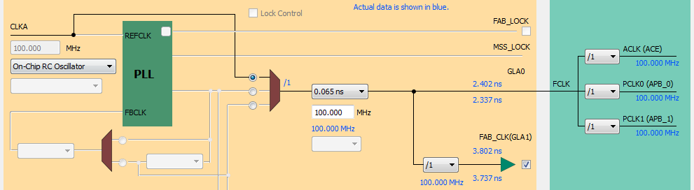
Select OK to close the clock
configurator window.
We will not need the other
default enabled components. Disable them by unchecking all the
boxes.
Lastly, we will not need the
MSS_RESET_N system reset signal. Double click on RESET Management
box and disable " Enable Chip-level Reset" box.
With the andor_MSS tab
selected, save the file.
Select the andor tab. You
will notice that the andor_MSS_0 instance indicates it needs to be
updated.
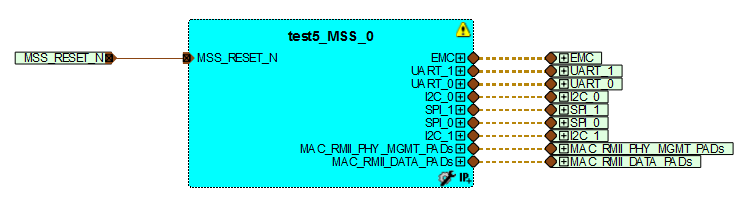
Select the instance, right
click and select
"Update Instance(s) with Latest Component". You
should now see the FABCLK
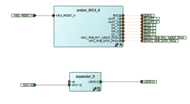
port on the andor_MSS_0 instance and the other ports removed.
Select the FABCLK port and
the clk input (2nd select is control and left click) of the myandor
module. While holding the mouse over one of the select ports, right
click and select connect. You final design should look like this.
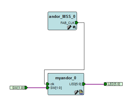
Make Sure the Root is Set
The
"Root" defines the high level design component. In this case, the
highest level design component is the andor project with andor_MSS_0
and myandor_0 as subcomponents or modules. Libero translates these
graphics representation to Verilog. The andor_MSS_0 component is a
module with one output port FAB_CLK and myandor_0 is a module with
inputs clik and SW[1:0] and LED[5:0] as outputs. The high level
component andor is then a module with inputs defined by the connectors
SW[1:0] and LED[5:0]. Make sure that andor is set as the root by
looking in the Design Hierarchy Tab. You should notice that it is in
bold. If andor_MSS_0 or myandor_0 is bold, right click on andor and set
it to root.
Generate
With the andor tab selected generate.
Add FPGA Pins
You will have to add the FPGA
pins for LED 3-5, so double click on Create/Edit IO Attributes
Implement-->Compile-->Constrain Place and Route in the Design
Flow window. Add the LED 3-5 pin and finish programing the FPGA using the
procedures detailed in the previous steps. See below for a quick reference to the FPGA pin numbers.
.
Testing the Design
Test your design on the kit.
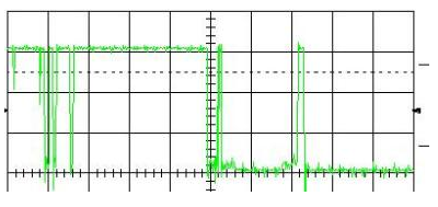
Hold down SW 1 and press SW 0 to reset the counter. Press SW 0 see see
the counter increment. You may notice that the more than one count may
occur when you press or release. . This is a consequence of
mechanical switch behavior called bounce. When a mechanical switch like
our pushbutton is pushed or released, it vibrates across the contact
points for a few milliseconds. Electrically this produces several
signal transitions. Consequently, several rising edges may occur with
each press or release. The following imagine is a time trace showing a
typical switch bounce. This is a consequence of pushing or releasing a
switch just once.
Switch
Bounce Trace
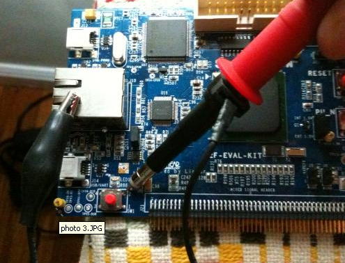
You can observe switch bounce with an oscilloscope. You will have to
have to set the scope to trigger for just one trace. Refer to the Lab
Instrument Introduction for more details. The switch can be probed
directly as shown in the following figure.
Probing
a Push Button Switch
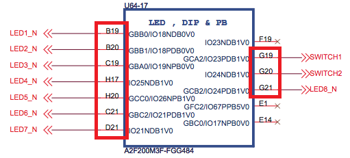
LED, SWITCH, USER I/O Pin-out
Quick Reference
Here are the pin numbers of the
SmartFusion chip that are connected
to the physical LED1-8, SW1,2 and user IO 1-5. The figures are specific
to the kit and can be found in the kit reference manual. http://www.actel.com/documents/A2F_EVAL_KIT_UG.pdf.
Note, the LED numbering in the following figure begins with one.
LED
and Pushbutton Switch FPGA Pin Numbers
USER I/O Pins. J22 at the top
of the header is the header number on
the physical Printed Circuit Board (PCB). It
is not the location of
pin J22. In fact, USER I/O 1
(pin J19) start is at that location.
User
IO Pin Header FPGA Pin Numbers
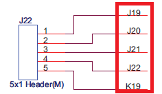 User IO Header
Common Tool Flow Pitfalls
- The following issues will be updated as
more are revealed. Check for new listings.
- If you do not explicitly make FPGA pin assignments to your high
level ports, Libero will assign arbitrary FPGA pin assignments to the
ports.
- If you select "Clean and Run All" by right clicking on Program
Device, your pin constraints will be removed and Libero will make
arbitrary FPGA pin assignments to the ports.
- The Design Flow window can take a few seconds to update after you
make a change. For example, if you make a change to one of your source
files the dependent Implementations such as Synthesis and Place
and Route should change from a completed process (green check mark) to
incomplete process (yellow triangle with exclamation) indicating the
source files are out of date with the current implementation.
- Sometimes
the pin assignments seems to change. It is prudent to check these if
you design mysteriously stops working. If this happens, all the
pin
assignments should change.
- Generally, the project (top level view) should always be the
declared as the ROOT. If it is one of the instances in the project, it
will not work or the porting will not work.