| Rule | Description | Lambda |
|---|---|---|
| DEEP | ||
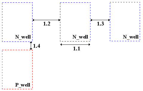
| 1.1 | Minimum width | 12 |
| 1.2 | Minimum spacing between wells at different potential | 18 |
| 1.3 | Minimum spacing between wells at same potential | 6 |
| 1.4 | Minimum spacing between wells of different type (if both are drawn) | 0 |
| Rule | Description | Lambda |
|---|---|---|
| DEEP | ||
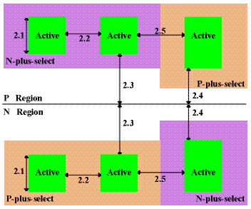
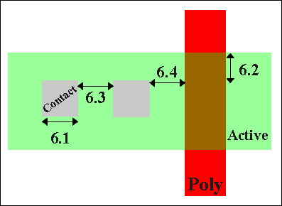
| 2.1 | Minimum width | 3 |
| 2.2 | Minimum spacing | 3 |
| 2.3 | Source/drain active to well edge | 6 |
| 2.4 | Substrate/well contact active to well edge | 3 |
| 2.5 | Minimum spacing between non-abutting active of different implant. Abutting active ("split-active") is illustrated under Layout Rules - Select. | 4 |
| Rule | Description | Lambda |
|---|---|---|
| DEEP | ||
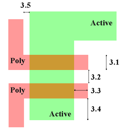
| 3.1 | Minimum width | 2 |
| 3.2 | Minimum spacing over field | 3 |
| 3.2.a | Minimum spacing over active | 4 |
| 3.3 | Minimum gate extension of active | 2.5 |
| 3.4 | Minimum active extension of poly | 4 |
| 3.5 | Minimum field poly to active | 1 |
| Rule | Description | Lambda |
|---|---|---|
| DEEP | ||
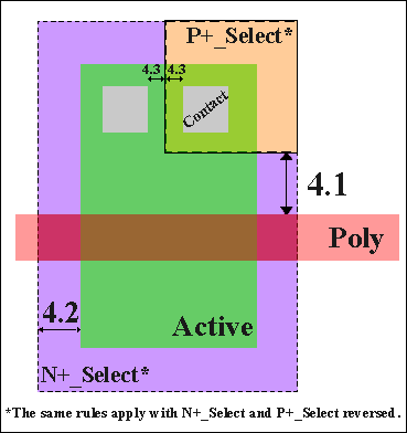
| 4.1 | Minimum select spacing to channel of transistor to ensure adequate source/drain width | 3 |
| 4.2 | Minimum select overlap of active | 2 |
| 4.3 | Minimum select overlap of contact | 1.5 |
| 4.4 | Minimum select width and spacing
(Note: P-select and N-select may be coincident, but must not overlap) (not illustrated) |
4 |
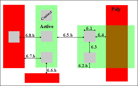
| Rule | Description | Lambda |
| DEEP | ||
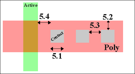
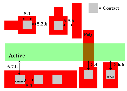
| 5.1 | Exact contact size | 2x2 |
| 5.2b | Minimum poly overlap | 1 |
| 5.3 | Minimum contact spacing | 4 |
| 5.4 | Minimum spacing to gate of transistor | 2 |
| 5.6.b | Minimum spacing to active (one contact) | 2 |
| 5.7.b | Minimum spacing to active (many contacts) | 3 |
 |
 |
|
|
 |
 |
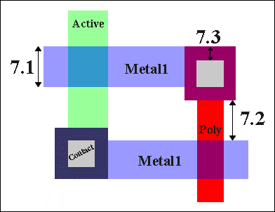
| Rule | Description | Lambda |
|---|---|---|
| DEEP | ||
| 7.1 | Minimum width | 3 |
| 7.2 | Minimum spacing | 3 |
| 7.3 | Minimum overlap of any contact | 1 |
| 7.4 | Minimum spacing when either metal line is wider than 10 lambda | 6 |
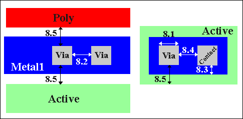
| Rule | Description | Lambda |
|---|---|---|
| DEEP | ||
| 8.1 | Exact size | 3 x 3 |
| 8.2 | Minimum via1 spacing | 3 |
| 8.3 | Minimum overlap by metal1 | 1 |
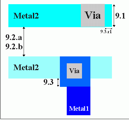
| Rule | Description | Lambda |
| DEEP | ||
| 9.1 | Minimum width | 3 |
| 9.2 | Minimum spacing | 4 |
| 9.3.r0 | Minimum overlap of via1 | 0 |
| 9.3.r1 | Minimum extension of via1 | 1 |
| 9.3.r2 | Minimum area | 25 (5x5) |
| 9.4 | Minimum spacing when either metal line is wider than 10 lambda | 8 |
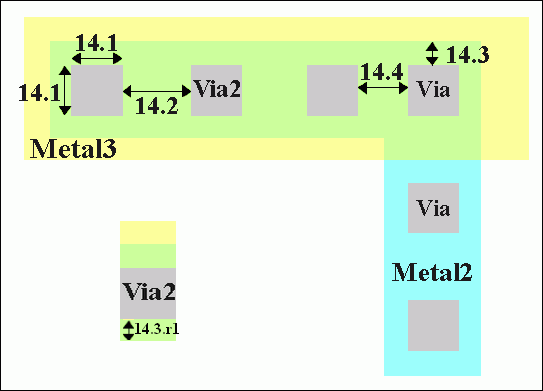
| Rule | Description | Lambda |
|---|---|---|
| DEEP | ||
| 14.1 | Exact size | 3x3 |
| 14.2 | Minimum spacing | 3 |
| 14.3.r0 | Minimum overlap by metal2 | 0 |
| 14.3.r0 | Minimum extension by metal2 | 1 |
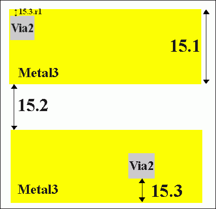
| Rule | Description | Lambda |
| DEEP | ||
| 15.1 | Minimum width | 3 |
| 15.2 | Minimum spacing to metal3 | 4 |
| 15.3.r0 | Minimum overlap of via2 | 0 |
| 15.3.r1 | Minimum extension of via2 | 1 |
| 15.3.r0 | Minimum area | 25 (5x5) |
| 15.4 | Minimum spacing when either metal line is wider than 10 lambda | 8 |