Other Support Staff:
|
Course Catalog:
|
|
DCO Support:
jvanlav@eecs.umich.edu |
Contact Joel VanLaven (staff) for major CAD tool issues. |
|
|
Computer Support:
CAEN hotline |
Contact them at 763-5041, in person at room 1315 of the Duderstadt Center, or through their web site for
printer/network problems. |
|
Course
Description: VLSI Design I (4 credits) Syllabus
Course Info
- Design techniques for rapid implementations of very large-scale
integrated (VLSI) circuits, MOS technology and logic.
- Structured design.
- Design rules, layout procedures.
- Design aids: layout, design rule checking, logic and circuit simulation.
- Timing and testability.
- Architectures for VLSI.
- Projects to develop and layout circuits.
|
Course Objectives:
|
Assignments:
|
This course introduces mask-level
integrated circuit design. Correct engineering design methodology is emphasized. Topics covered
in lectures include: CMOS processes, mask layout methods and design rules; circuit characterization
and performance estimation; design for testability; and CMOS subsystem and system design.
Lab: This is a project-oriented course in which you will design a
modest-sized CMOS integrated circuit. Except for the tutorials at
the beginning of the semester, no specific lab times are scheduled, and
you can work at your convenience. CAEN Labs are open 24 hours a day.
|
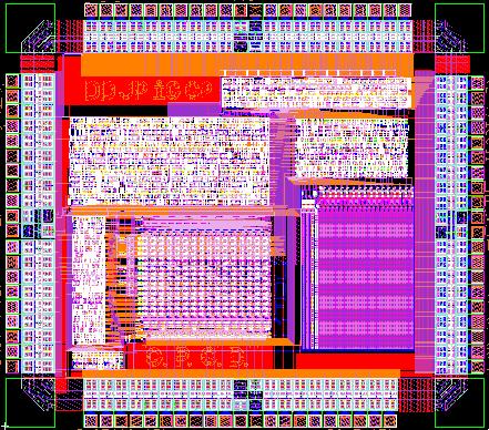
The term project involves the design
of a 16-bit RISC microprocessor. The initial cell designs (CAD assignments 1 & 2) probably will not be used in the final project
and must be done individually. You are encouraged to interact with others, but until you are asked to form
teams, the work on your cell designs, simulations, etc., must be your own. There is an initial, individual homework
assignment to ensure that all students have the prerequisite digital IC design knowledge needed to succeed in EECS 427.
The final project will be done in teams of four. The project must be completed, and you must submit a
final report in the format specified. Within the constraints of available funding, eligible projects will
be fabricated through the MOSIS service. If your project is fabricated, it must be tested; you can get
credit for testing it in EECS 579 or as a directed study project. You are encouraged to enter your design
in the DAC Student Design Contest.
|
Prerequisites:
|
Exams:
|
|
EECS 270 and EECS 312. Students are expected to know logic design, transistor-level circuit design
(especially static CMOS), and device physics. Some background in computer architecture is helpful
(EECS 370), but not required. |
There will be 90 minute (in-class) quizzes approximately every 6 weeks during the semester (2 quizzes total). |
Textbook:
|
Grading Policy:
|
Jan Rabaey, Anantha Chandrakasan, and Borivoje Nikolic, Digital
Integrated Circuits: A Design Perspective, 2nd edition,
Prentice Hall, 2003.
We will also be pulling material from the following texts:
N. Weste and D. Harris, CMOS VLSI Design: A Circuits and Systems Perspective,
3rd edition, Addison-Wesley, 2005.
Design of High-Performance Microprocessor Circuits, edited by A. Chandrakasan,
W. Bowhill, and F. Fox, IEEE Press, 2001.
Another useful circuit design reference is:
D.A. Hodges, H.G. Jackson, and R.A. Saleh, Analysis and Design of Digital Integrated Circuits
in Deep Submicron Technology, 3rd edition, McGraw Hill, 2004.
|
Homeworks (including project presentation): 10%
CAD assignments: 35%
Quizzes: 24% (12% each)
Final project, report, and individual contributions: 31%
Late policies:
CAD assignments will be submitted electronically and are due at 7pm on the due date
(except CAD9). Be sure to do your design work in the class directory so that we will
have access to it. Do not change the access rights to your class directory. Do not modify
submitted files until you get email to say that they have been graded. Late penalties are
25% if the time stamp is from 7:01pm of the due date to 7:00pm of the next day, 50% from
7:01pm of the day after the due date to 7:00pm of the following day, and no credit if turned
in later than that. Note that late penalties are applied only to those portions of the
assignment that are finished late. For example, if the schematic and functional verification
was completed on time but layout was late, only the layout portion will be subject to the late penalty.
Written homework is due in class, at the beginning of lecture. A penalty of 30%
will be assessed if the homework is turned in within 24 hours of the due date. After this point,
no late homeworks will be accepted.
Engineering
Honor Code |