EECS 427 - VLSI Design I : Fall 2007
| Home | Info | Schedule | Lectures | Assignments | Handouts | Solutions |
|---|
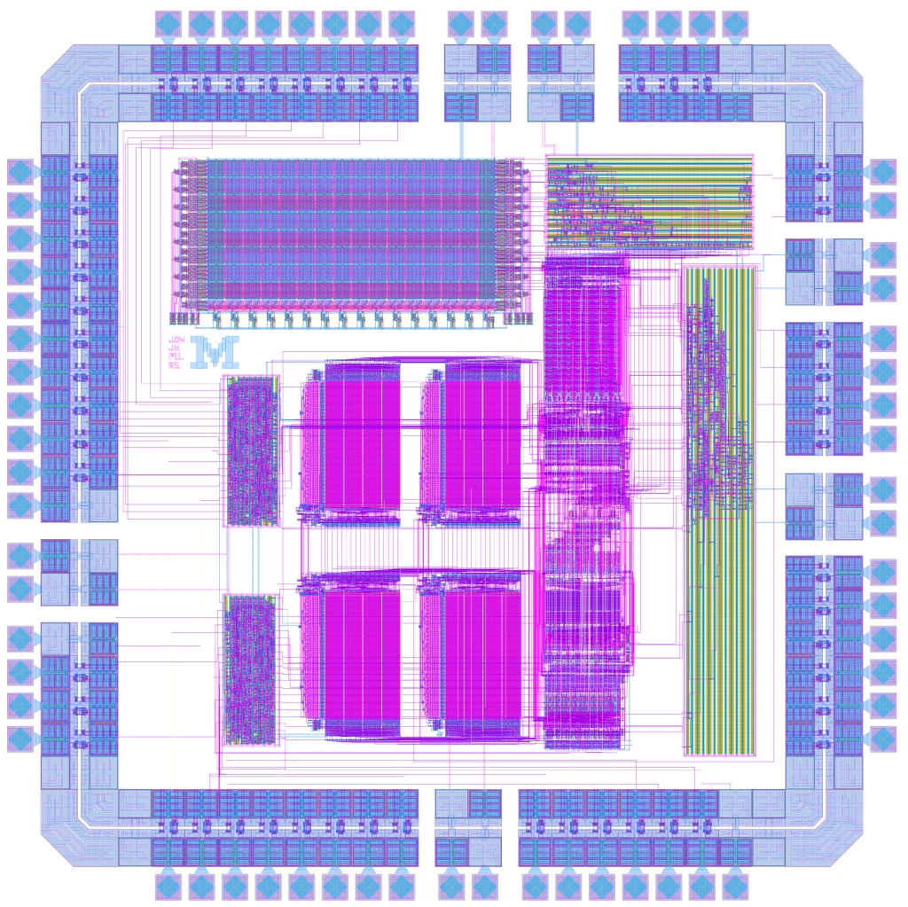
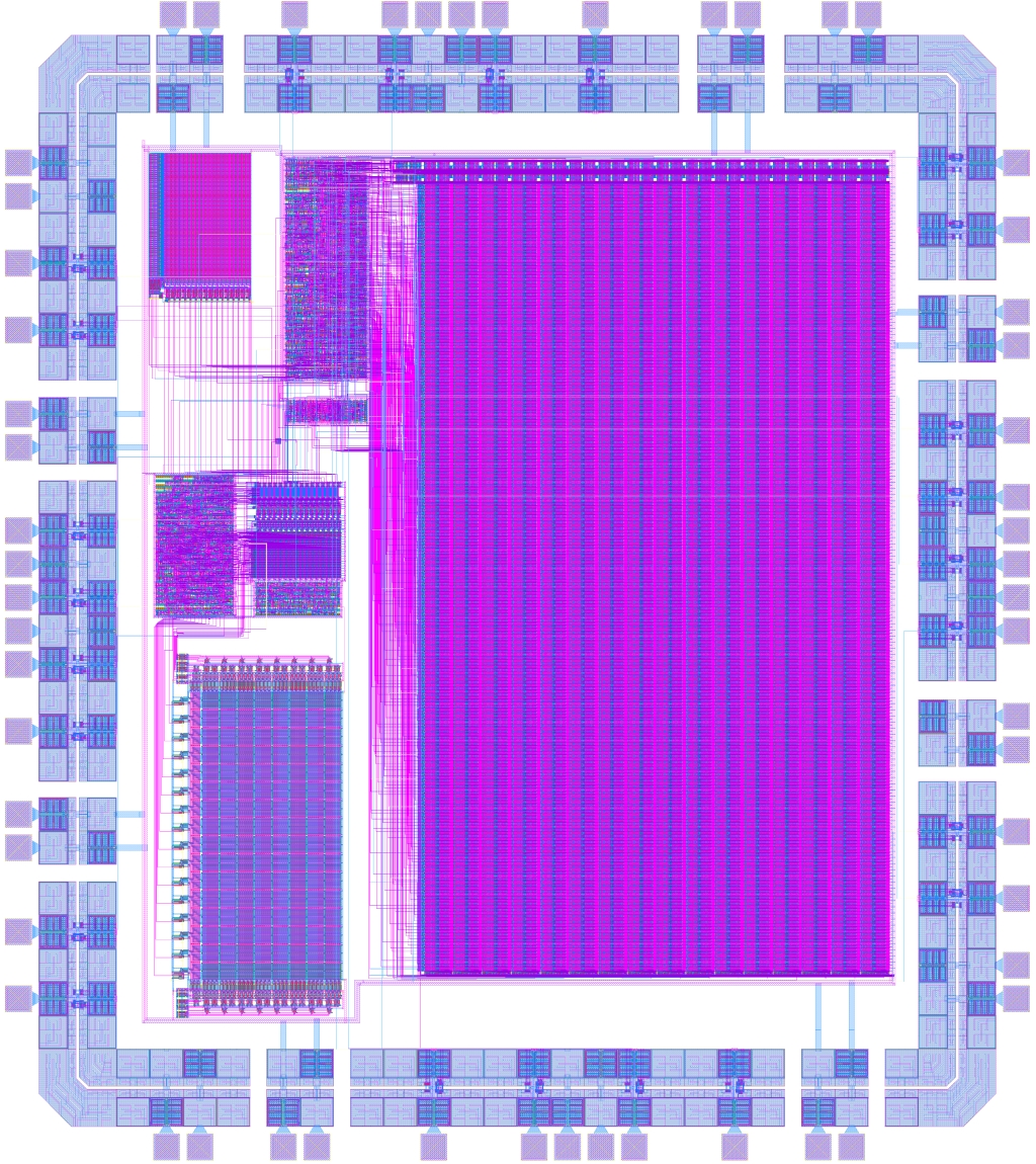
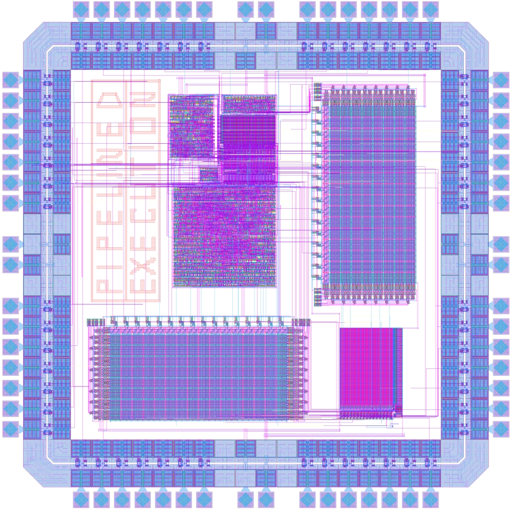
| Binary Fission | Kikloma | Pipelined Execution | Micronauts |
|---|---|---|---|
 |
 |
 |
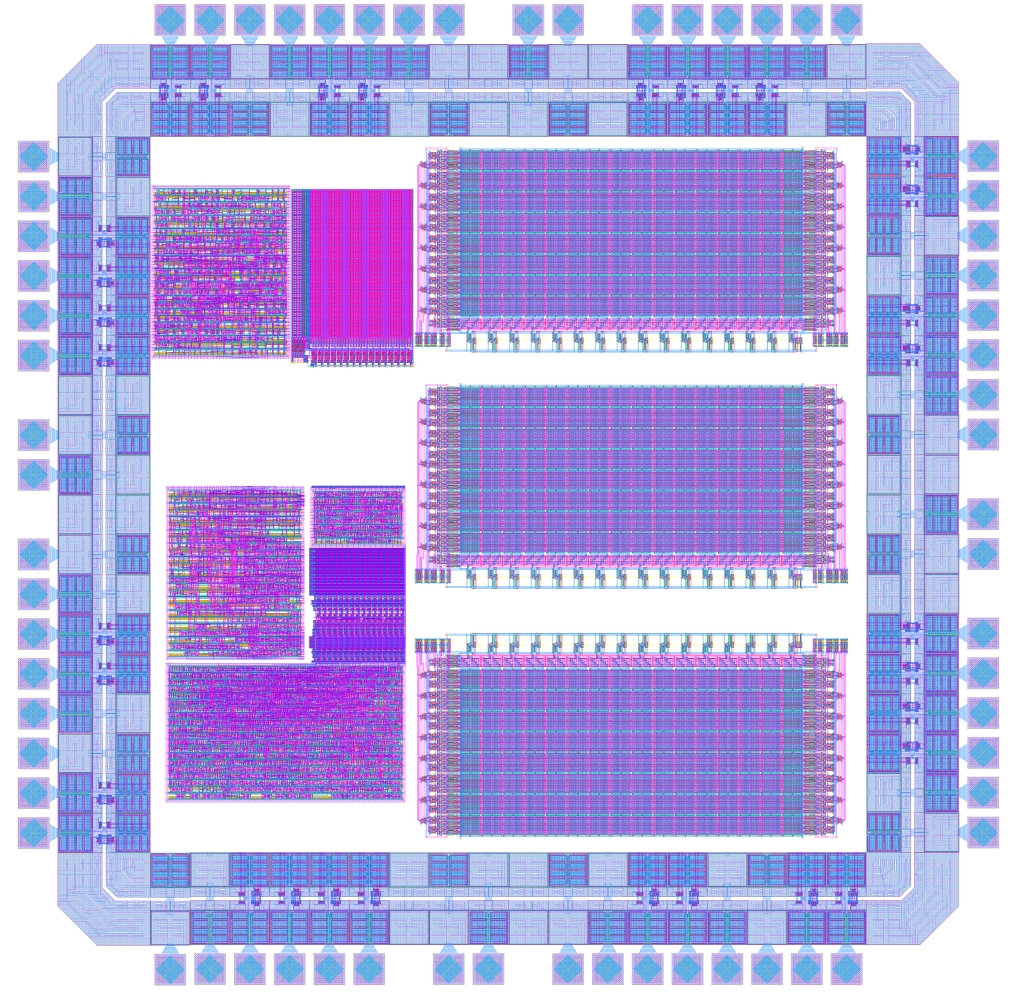 |
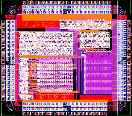
| bfissionbig.png | kiklomabig.png | pebig.png | micronautsbig.png |
 General Purpose Groundskeeping Device, by Doug Densmore, Irena Gershkovich, Jennifer Pann and Greg Pezda, Fall 2000. |
|
||||||||||
|---|---|---|---|---|---|---|---|---|---|---|---|
ANNOUNCEMENTS
The following code is the correct code to place in your .cshrc. Sorry for confusion. You can copy and paste this for ease of use.if ($?prompt) then if (! -f /afs/umich.edu/class/eecs427/tsmc25/cshrc) then gettokens endif source /afs/umich.edu/class/eecs427/tsmc25/cshrc endif |
On HW1, ΦF = -0.3 Also, all values for k were given in mA but should be in μA |
All office hours the week of Jan 15-19 will be with Joel (Vishvesh is out of town) and Tuesday Jan 16 the office hours will be 2:00-4:00 instead of 11:00-1:00 (Joel has a meeting) |
|---|---|---|
| On HW1 Question 3: One way to estimate the slew is to assume a voltage current relationship that is perfectly linear out from the origin and is perfectly flat after Vd-sat. This way the analysis for the 50% delay will not change( Use the current source model) and for the t_rise and t_fall just analyze the transistor in the 2 simplified linear regions. For t_fall analysis should be from 2.25 to Vd-sat as one section and Vd-sat to 0.25 as another section. |
| Other Support: | Course Catalog: |
|---|---|
|
Computer Support: CAEN hotline Contact them at 763-5041, in person at room 1315 of the Duderstadt Center, or through their web site for printer, network, machine, account, or similar problems in the CAEN labs |
Course
Description: VLSI Design I (4 credits)
|
| Course Objectives: | Assignments: |
| This
course introduces mask level integrated circuit design. Correct
engineering design methodology is emphasized. Topics covered in
lectures include: CMOS processes, mask layout method and design
rules; circuit characterization and performance estimation; design for
testability; and CMOS subsystem and system design. Lab: This is a project-oriented course in which you will design a modest-sized CMOS integrated circuit. Except for the short courses at the beginning of the semester, no specific lab times are scheduled, and you can work at your convenience. CAEN Labs are open 24 hours a day. |
The term project involves the
design of a 16-bit RISC microprocessor. The initial cell designs
probably will not be used in the final project and must be done
individually. You are encouraged to interact with others, but
until you are asked to form teams, the work on your cell designs, simulations,
etc., must be your own. There is an initial homework assignment to
ensure that all students have the prerequisite digital IC design
knowledge to succeed in EECS 427. The final project will be done in teams of four. The project must be completed, and you must submit a final report in the format specified. Within the constraints of available funding, eligible projects will be fabricated through the MOSIS service. If your project is fabricated, it must be tested; you can get credit for testing it in EECS 579 or as a directed study project. You are encouraged to enter your design in the DAC Student Design Contest. |
| Textbook: | Prerequisites: |
| Jan Rabaey, Anantha Chandrakasan, and Borivoje Nikolic, Digital Integrated Circuits: A Design Perspective, second edition, Prentice Hall, 2003. | EECS 270 and EECS 312. Students are expected to know logic design, transistor-level circuit design (especially static CMOS), and device physics. Some background in computer architecture is helpful (EECS 370), but not required. |
| Grading Policy: | Other Links: |
|
Homeworks (including project presentation): 10% CAD assignments: 35% Quizzes: 24% (8% each) Final project, report, and individual contributions: 31% Late policies: CAD assignments will be submitted electronically and are due at 7pm on the due date (except CAD9). Be sure to do your design work in the class directory so that we will have access to it. Do not change the access rights to your class directory. Do not modify submitted files until you get email to say that they have been graded. Late penalties are 25% if the time stamp is from 7:01pm of the due date to 7:00pm of the next day, 50% from 7:01pm of the day after the due date to 7:00pm of the following day, and no credit if turned in later than that. Note that late penalties are applied only to those portions of the assignment that are finished late. For example, if the schematic and functional verification was completed on time but layout was late, only the layout portion will be subject to the late penalty. Written homework is due in class, at the beginning of lecture. A penalty of 30% will be assessed if the homework is turned in within 24 hours of the due date. After this point, no late homeworks will be accepted. Engineering Honor Code |
Information on Chip Fabrication at USC Information Sciences Institute (ISI) - MOSIS
(MOS Implementation Service) Homepage
DAC Student Design Contest VLSI Graduate Study at the University of Michigan ICMaster - searchable parts database OpenCores - open source hardware IP University of Idaho's VLSI Links. MIT's Semiconductor Subway. CMP (Circuits Multi-Projets): France's version of MOSIS. |